|![[Search]](https://talks.cam.ac.uk/images/search.gif?1209136071) |
|![[A-Z Index]](https://talks.cam.ac.uk/images/az.gif?1209136071) |
|![[Contact]](https://talks.cam.ac.uk/images/contact.gif?1209136071)
| COOKIES: By using this website you agree that we can place Google Analytics Cookies on your device for performance monitoring. | ![[Talks.cam]](https://talks.cam.ac.uk/images/talkslogosmall.gif?1209136071) |
University of Cambridge > Talks.cam > Semiconductor Physics Group Seminars > Transport of modulation-doped Al0.2Ga0.8Sb/GaSb heterojunctions
Transport of modulation-doped Al0.2Ga0.8Sb/GaSb heterojunctionsAdd to your list(s) Download to your calendar using vCal
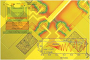
If you have a question about this talk, please contact Dr Joanna Waldie. GaSb has a number of known applications, primarily in optoelectronics, such as infrared detectors, thermophotovoltaic converters and LED ’s. However, the transport properties of this material (both the standard p-type and more uncommon n-type) have generally been restricted to bulk GaSb. GaSb also has a lower electron effective mass than it’s better-studied counterpart, GaAs, however it has a large number of defects regardless of growth method, producing a high acceptor background. Theoretical transport results were produced using Nextnano software [1], with the aim of measuring confined two-dimensional electron gas devices (a system not previously reported in GaSb). GaSb/Al0.2Ga0.8Sb heterostructures were grown at Lancaster University by molecular beam epitaxy, with Hall bars of varying sizes subsequently fabricated. Measurements of these devices yielded a higher accepting background than intended and ultimately resulted in p-type devices. I will discuss the theoretical and experimental results of these devices, as well as subsequent growth trials of this material, the problems we faced and how we are combating them. [1] S. Birner et al., Acta. Phys. Polonica. A 110 , 111, (2006). This talk is part of the Semiconductor Physics Group Seminars series. This talk is included in these lists:
Note that ex-directory lists are not shown. |
Other listsExperimental Psychology Datalog for Program Analysis: Beyond the Free Lunch Things that Matter 1400-1900Other talksQuantum geometry from the quantisation of gravitational boundary modes on a null surface Babraham Lecture - Understanding how the p53 onco-suppressor gene works: hints from the P2X7 ATP receptor Developmental cognitive neuroscience Babraham Lecture - The Remote Control of Gene Expression THE MATHEMATICAL MAGIC OF MIXED REALITY Statistical analysis of biotherapeutic datasets to facilitate early ‘Critical Quality Attribute’ characterization. |

 Laura Hanks, University of Lancaster
 Wednesday 25 October 2017, 14:15-15:00